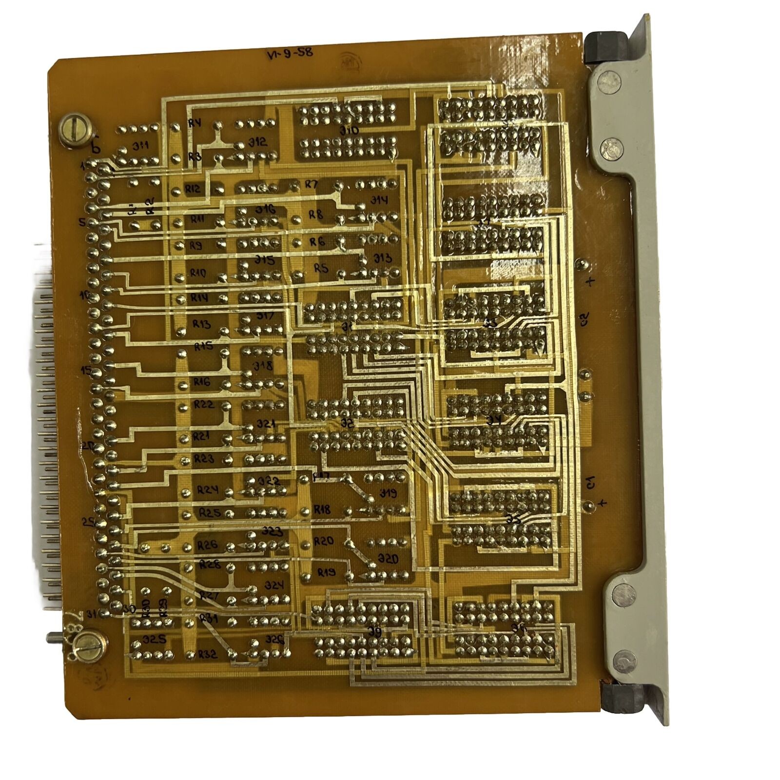
A printed circuit board (PCB), is the backbone of modern electronics. It’s a board that uses conductive tracks, pads and other features etched from one or more sheet layers of copper laminated onto and/or between sheet layers of a non-conductive substrate. PCBs mechanically support and electrically connect electronic components using conductive pathways, or traces, etched from copper sheets laminated onto a non-conductive substrate.
PCBs are essential because they provide a structured and reliable way to connect electronic components. Without PCBs, electronics would be a chaotic mess of wires and components.
All PCBs are built from alternating layers of conductive copper with layers of electrically insulating material. Conductive features on printed circuit boards include copper traces, pads, and conductive planes. The mechanical structure is made up of the insulating material laminated between the layers of conductors. The overall structure is plated and covered with a non-conductive solder mask, and silk screen is printed on top of the solder mask to provide a legend for electronic components. After these fabrication steps are completed, the bare board is sent into printed circuit board assembly, where components are soldered to the board and the PCBA can be tested.
The inner copper layers are etched, leaving the intended traces of copper for connecting components in the circuit board. Multiple etched layers are laminated in succession until the printed circuit board stack-up is complete. This is the overall process used in PCB design fabrication, where the bare board is formed before passing through a printed circuit board’s assembly process.
A Brief History of PCBs
To fully appreciate the intricacies of PCB design, it’s helpful to understand their evolution.
In the early days of electronics, components were connected using point-to-point wiring. This method was time-consuming, prone to errors, and difficult to maintain. As electronics became more complex, a better solution was needed.
Early PCBs, made from materials like Bakelite, used wires to connect integrated circuits (ICs) and discrete components. These boards were cumbersome, difficult to debug, and unreliable due to manual soldering. Manufacturing was slow and complex, involving manually soldering multiple components and their wired connections.
Today, PCBs boast miniaturized components, including tiny ICs, passive components, and advanced chips with high pin counts. Copper connections are deposited directly onto insulating substrates. Modern devices utilize high-density interconnect (HDI) designs with numerous connections and electrical interfaces, enabling smartphones, heart rate monitors, and even rockets.
Common Types of PCBs
While rigid PCBs are the most prevalent, various types cater to specific applications. These include:
- Single-Layer PCBs: These PCBs have a single layer of conductive material on one side of the board. They are simple and cost-effective, suitable for basic electronic devices.
- Double-Layer PCBs: These PCBs have a layer of conductive material on both sides of the board, allowing for more complex circuits.
- Multilayer PCBs: These PCBs have three or more layers of conductive material, separated by insulating layers. They are used in complex electronic devices, such as computers and smartphones.
- Flexible PCBs: These PCBs are made from flexible materials, allowing them to be bent or folded. They are used in applications where space is limited or where the board needs to conform to a curved surface.
- Rigid-Flex PCBs: These PCBs combine rigid and flexible sections, offering a balance of flexibility and support.
Modern ECAD software empowers designers to create any of these boards, provided the correct PCB design rules are applied.
Understanding PCB Structure and Its Applications
The stack-up, or the arrangement of layers, significantly impacts a PCB’s performance. Alternating layers of conductive and insulating materials, along with core and prepreg dielectrics, determine reliability and signal/power integrity. High-reliability applications, such as military and medical devices, demand careful material selection. Telecom systems might require low-loss PTFE laminate in a compact form factor.
A typical PCB stack-up consists of a 4-layer structure with internal plane layers for ground and power. This configuration suits IoT devices, embedded systems, and designs using high-speed protocols. Internal planes ensure power integrity and shield against external EMI, while providing a consistent reference for controlled impedance signals.
High-Density Interconnect (HDI) PCBs
Advanced devices use high-density interconnect (HDI) design practices, enabling extremely small feature sizes. These PCBs are deployed in systems requiring numerous components and connections. Common applications include:
- Smartphones and mobile devices
- Data center architecture (e.g., server motherboards)
- Add-in cards for servers and embedded computers
- Miniature medical wearables and implants
Ball grid array (BGA) packaging drives HDI design and manufacturing, allowing a high number of I/O pins in a small package. BGA packages are key to miniaturization, with consumer products often utilizing custom processors in BGA packages.
Ultra-High Density Interconnect (UHDI) PCBs
UHDI PCBs represent the next evolution, converging with component packaging. Semiconductor chips are placed on an IC substrate, facilitating interconnections between the chip’s electrical contacts and the PCB. UHDI PCBs and IC substrates share similar feature sizes and manufacturing processes.
Producing UHDI PCBs pushes manufacturing limits, requiring additive processes where traces and vias are formed through metal deposition rather than subtractive etching. These PCBs will drive the most advanced systems operating at the highest data rates. Despite the different production processes, designing UHDI PCBs is similar to designing conventional PCBs.
Starting a New PCB Design
Creating a PCB involves several stages, typically utilizing ECAD software. The process begins with electrical drawings and concludes with manufacturing file preparation. Key steps include:
- Schematic Capture: Creating a circuit diagram representing the electrical connections between components.
- PCB Layout: Arranging components and routing traces on the PCB.
- Gerber Generation: Creating files used by manufacturers to fabricate the PCB.
To streamline this process, designers need design software with an intuitive user interface and a complete set of PCB design features.
Streamlining PCB Design with Altium Designer
The best ECAD software should be user-friendly and feature-rich. Altium Designer integrates all necessary tools into a single program, eliminating the need for external software.
Altium Designer is consistently praised for its ease of use, making it suitable for both novice and experienced designers. Altium Designer on Altium 365 enhances integration within the electronics industry, allowing designers to work remotely and achieve greater efficiency.
This overview scratches the surface of Altium Designer’s capabilities. Start your free trial of Altium Designer + Altium 365 today and experience the power of unified PCB design.