What is a PCB? Printed Circuit Boards are the unsung heroes of modern electronics, enabling countless devices we rely on daily. At WHAT.EDU.VN, we aim to demystify PCBs, exploring their definition, functionality, and applications. Learn all about these critical components, including PCB materials, design, and manufacturing, and discover why they’re vital to our technological world.
1. Understanding the Fundamentals: What is a PCB (Printed Circuit Board)?
A Printed Circuit Board (PCB) is more than just a green board filled with wires; it’s the foundation upon which electronic devices are built. It serves as the backbone, providing both electrical connections and mechanical support for components. In essence, it’s a meticulously designed platform that enables the seamless operation of everything from smartphones to complex industrial machinery.
At its core, a PCB is a laminate structure comprised of alternating layers of conductive material, typically copper, and insulating material, like fiberglass epoxy. The conductive layers are etched to create intricate pathways, known as traces, which electrically connect various electronic components. These components, such as resistors, capacitors, integrated circuits (ICs), and connectors, are then soldered onto the board, completing the circuit.
A cross-sectional view of a PCB highlights the layered structure and the integration of various components.
PCBs are crucial because they offer a reliable, organized, and compact way to assemble complex electronic circuits. Before PCBs, electronics were built using point-to-point wiring, a laborious and error-prone process. PCBs streamlined manufacturing, improved reliability, and enabled the miniaturization of electronic devices.
Want to dive deeper and ask specific questions about PCB design or troubleshooting? Visit WHAT.EDU.VN and get free answers from experts in the field!
2. A Brief History: From Wires to Printed Circuits
The journey of PCBs began in the early 20th century as a response to the growing complexity of electronic circuits.
2.1. Early Days of Electronics: The Era of Point-to-Point Wiring
Before the advent of PCBs, electronic circuits were assembled using point-to-point wiring. This involved connecting electronic components together using wires, with each connection made individually. While this method worked for simple circuits, it became increasingly impractical as circuits grew more complex. The sheer number of wires resulted in tangled messes, making troubleshooting difficult and increasing the likelihood of errors.
An example of an early electronic system using point-to-point wiring, showcasing the complex web of connections.
2.2. The Birth of the PCB: A Revolution in Electronics
The concept of the PCB emerged as a solution to the limitations of point-to-point wiring. The first PCBs were simple boards with conductive pathways printed or etched onto their surface. This innovation allowed for a more organized and efficient way to connect electronic components.
2.3. Key Milestones in PCB Development
- 1936: Paul Eisler patented the first PCB technology while working on a radio set.
- 1950s: PCBs began to be widely adopted in commercial electronics.
- 1960s: The introduction of integrated circuits (ICs) further fueled the growth of PCB technology, as these complex components required more sophisticated interconnection methods.
- Late 20th Century: Advancements in materials, manufacturing processes, and design software led to the development of high-density, multi-layer PCBs.
2.4. PCBs Today: Powering the Modern World
Today, PCBs are ubiquitous in electronic devices, from smartphones and computers to automobiles and medical equipment. They have become an indispensable part of modern technology, enabling the development of smaller, faster, and more reliable electronic systems.
Do you have more questions about the evolution of PCB technology? Get them answered for free at WHAT.EDU.VN. We provide a platform to ask any question and receive expert opinions.
3. Delving Deeper: Types of PCBs and Their Applications
PCBs come in various forms, each tailored for specific applications and performance requirements. Let’s explore some of the most common types:
3.1. Single-Sided PCBs: Simplicity and Cost-Effectiveness
Single-sided PCBs have a conductive layer on only one side of the board. They are the simplest and most cost-effective type of PCB, suitable for low-density circuits and basic electronic devices.
- Applications: Simple consumer electronics, LED lighting, calculators.
3.2. Double-Sided PCBs: Increased Complexity and Versatility
Double-sided PCBs have conductive layers on both sides of the board, allowing for more complex circuits and higher component density. They often include plated through-holes (PTH) to connect circuits on opposite sides.
- Applications: Power supplies, audio amplifiers, industrial controls.
3.3. Multi-Layer PCBs: High-Density Interconnect Solutions
Multi-layer PCBs consist of three or more conductive layers, separated by insulating layers. These boards offer the highest level of complexity and component density, enabling the design of sophisticated electronic devices.
- Applications: Computers, smartphones, aerospace, medical imaging equipment.
3.4. Flexible PCBs: Adapting to Complex Geometries
Flexible PCBs are made from flexible substrates, such as polyimide film. They can be bent or folded to fit into tight spaces or conform to complex shapes.
- Applications: Wearable electronics, automotive sensors, medical devices.
3.5. Rigid-Flex PCBs: Combining Flexibility and Rigidity
Rigid-flex PCBs combine rigid and flexible sections in a single board. This allows for the integration of flexible circuits into rigid structures, offering both flexibility and mechanical support.
- Applications: Cameras, aerospace electronics, military equipment.
3.6. Aluminum-Backed PCBs: Enhanced Thermal Management
Aluminum-backed PCBs have a layer of aluminum laminated to the back of the board. The aluminum layer acts as a heat sink, dissipating heat away from electronic components.
- Applications: High-power LED lighting, power amplifiers, automotive electronics.
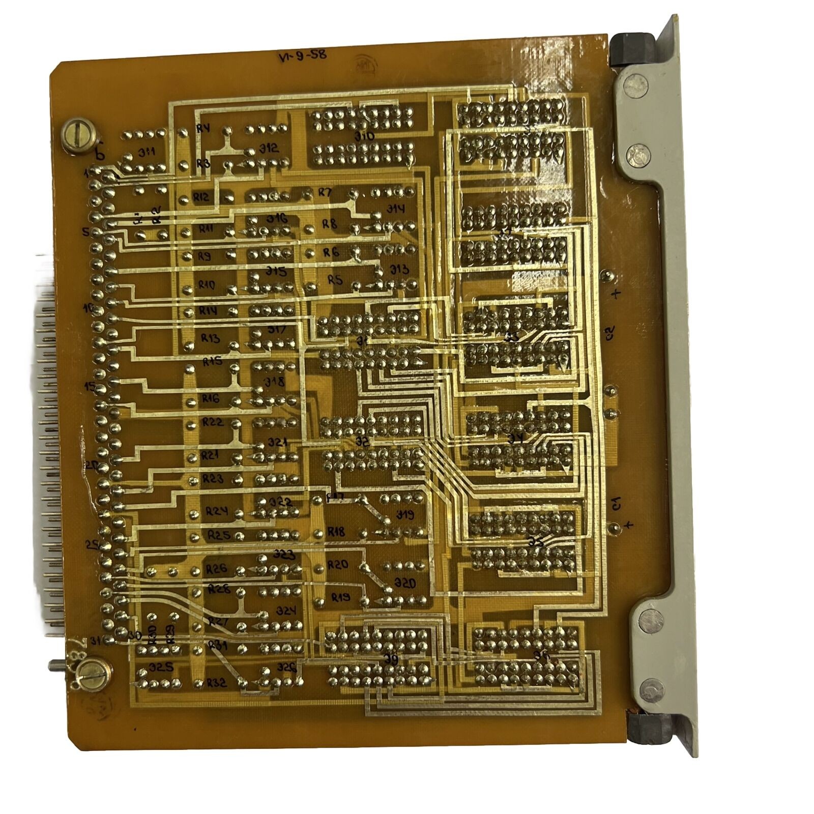
An older circuit board showcasing through-hole components, a common feature in earlier PCB designs.
Need help selecting the right type of PCB for your project? Ask the experts at WHAT.EDU.VN! Our free Q&A platform provides valuable insights and personalized advice.
4. Diving into the Anatomy: Key Components of a PCB
A PCB is a complex assembly, with each component playing a crucial role in its functionality. Understanding these components is essential for anyone involved in PCB design, manufacturing, or repair.
4.1. Substrate: The Foundation of the PCB
The substrate is the base material of the PCB, providing mechanical support and electrical insulation. Common substrate materials include:
- FR-4: A fiberglass epoxy laminate, offering a good balance of cost, performance, and manufacturability.
- CEM-1: A paper epoxy laminate, less expensive than FR-4 but with lower performance.
- Polyimide: A high-performance polymer with excellent thermal and electrical properties, used in flexible PCBs and high-temperature applications.
- PTFE (Teflon): A low-loss dielectric material, ideal for high-frequency applications.
4.2. Copper Layers: The Electrical Pathways
Copper layers provide the conductive pathways for electrical signals and power. These layers are etched to create traces, pads, and planes.
- Traces: Narrow conductive paths that connect electronic components.
- Pads: Small areas of copper used for soldering components to the board.
- Planes: Large areas of copper used for power distribution or grounding.
4.3. Solder Mask: Protecting the Copper
The solder mask is a protective coating applied to the PCB to prevent solder from bridging between traces and pads during soldering. It also protects the copper from oxidation and corrosion. The solder mask is typically green but can also be other colors.
4.4. Silkscreen: Identifying Components and Markings
The silkscreen is a layer of ink printed on the PCB to identify components, provide polarity markings, and display other information. It is typically white or yellow.
4.5. Plated Through-Holes (PTH): Connecting Layers
Plated through-holes (PTH) are holes drilled through the PCB and plated with copper to connect circuits on different layers. They are used to mount through-hole components and provide electrical connections between layers.
4.6. Surface Mount Pads: Connecting SMD Components
Surface mount pads are flat pads of copper on the surface of the PCB, designed for soldering surface mount devices (SMD).
A modern PCB showcasing surface mount device (SMD) components and the green solder mask layer.
Still confused about PCB components? Ask the experts at WHAT.EDU.VN for a simplified explanation! Get free, easy-to-understand answers to all your electronics questions.
5. The Manufacturing Process: From Design to Reality
Creating a PCB is a multi-step process that requires specialized equipment and expertise.
5.1. Design and Layout: Creating the Blueprint
The first step is to design the PCB layout using ECAD (Electronic Computer-Aided Design) software. This involves placing components, routing traces, and defining the layer stackup.
5.2. Film Generation: Preparing the Artwork
Once the design is complete, the ECAD software generates films, which are used to create the artwork for each layer of the PCB.
5.3. Imaging: Transferring the Design to the Copper
The artwork is then used to image the copper layers of the PCB. This involves coating the copper with a photoresist, exposing it to UV light through the artwork, and then developing the resist to reveal the areas to be etched.
5.4. Etching: Removing Unwanted Copper
The exposed copper is then etched away using a chemical etchant, leaving the desired traces, pads, and planes.
5.5. Drilling: Creating Holes for Components and Connections
Holes are drilled through the PCB to accommodate through-hole components and create vias for connecting different layers.
5.6. Plating: Connecting the Layers
The drilled holes are then plated with copper to create plated through-holes (PTH), which provide electrical connections between layers.
5.7. Solder Mask Application: Protecting the Copper
The solder mask is applied to the PCB to protect the copper and prevent solder bridging.
5.8. Silkscreen Printing: Adding Markings and Identification
The silkscreen is printed on the PCB to identify components and provide other markings.
5.9. Testing: Ensuring Quality and Functionality
The finished PCB is then tested to ensure that it meets the design specifications and functions correctly.
5.10. Assembly: Adding the Components
Finally, the electronic components are soldered to the PCB, either manually or using automated assembly equipment.
Want a more detailed explanation of the PCB manufacturing process? Ask your questions at WHAT.EDU.VN and receive clear, concise answers from experienced professionals.
6. Understanding PCB Stack-Up: The Key to Performance
The stack-up, or the arrangement of layers in a PCB, is crucial to its performance. Proper stack-up design can improve signal integrity, reduce EMI, and enhance power distribution.
6.1. Key Considerations for Stack-Up Design
- Signal Layers: Layers dedicated to routing high-speed signals.
- Power Planes: Layers dedicated to distributing power to the components.
- Ground Planes: Layers dedicated to providing a stable ground reference.
- Dielectric Materials: The insulating materials between the layers, which affect signal speed and impedance.
- Layer Thickness: The thickness of the copper and dielectric layers, which affects impedance and signal propagation.
6.2. Common Stack-Up Configurations
- 2-Layer Stack-Up: Suitable for simple circuits with low-speed signals.
- 4-Layer Stack-Up: A common configuration for general-purpose circuits, with two signal layers, a power plane, and a ground plane.
- 6-Layer Stack-Up: Provides better signal integrity and EMI performance compared to a 4-layer stack-up.
- 8-Layer Stack-Up and Higher: Used in high-speed, high-density applications requiring excellent signal integrity and EMI performance.
An example of a PCB stack-up design created using Altium Designer, showing the arrangement of different layers.
Confused about stack-up design? Get free guidance from PCB experts at WHAT.EDU.VN! Ask your specific questions and receive tailored advice.
7. Exploring High-Density Interconnect (HDI) PCBs: The Future of Miniaturization
High-Density Interconnect (HDI) PCBs represent the cutting edge of PCB technology, enabling the design of extremely compact and high-performance electronic devices.
7.1. What Makes a PCB an HDI PCB?
HDI PCBs are characterized by:
- Fine Lines and Spaces: Narrower traces and smaller spaces between traces, allowing for higher component density.
- Microvias: Small vias with a diameter of 0.006 inches (150 microns) or less, used to connect layers.
- Sequential Lamination: The process of adding layers to the PCB one at a time, allowing for the creation of complex interconnect structures.
- High Layer Count: HDI PCBs often have a higher layer count than conventional PCBs.
7.2. Applications of HDI PCBs
- Smartphones and Mobile Devices: HDI PCBs are essential for fitting complex electronics into small form factors.
- Wearable Electronics: Smartwatches, fitness trackers, and other wearable devices rely on HDI PCBs for their compact size and high performance.
- Medical Devices: HDI PCBs are used in medical implants, diagnostic equipment, and other medical devices requiring high reliability and miniaturization.
- Aerospace and Defense: HDI PCBs are used in aerospace and defense applications requiring high performance and reliability in harsh environments.
7.3. Benefits of HDI PCBs
- Increased Component Density: Allows for more components to be placed on the PCB.
- Improved Signal Integrity: Reduces signal reflections and crosstalk, improving signal quality.
- Reduced Size and Weight: Enables the creation of smaller and lighter electronic devices.
- Enhanced Thermal Performance: Improves heat dissipation, increasing the reliability of the device.
Want to know if HDI PCB technology is right for your next project? Get expert advice at WHAT.EDU.VN. Ask any question and get free, informative answers.
8. Ultra-High-Density Interconnect (UHDI) PCBs: The Next Frontier
Ultra-High-Density Interconnect (UHDI) PCBs represent the next evolution in PCB technology, pushing the limits of miniaturization and performance.
8.1. Defining UHDI PCBs
UHDI PCBs take HDI technology to the next level, with even finer lines and spaces, smaller vias, and more advanced manufacturing processes.
8.2. Key Features of UHDI PCBs
- Extremely Fine Lines and Spaces: Trace widths and spaces below 25 microns.
- Laser-Drilled Microvias: Microvias with diameters less than 50 microns.
- Advanced Materials: Specialized dielectric materials with ultra-low losses.
- Additive Manufacturing: Processes that deposit conductive material instead of etching it away.
8.3. Applications of UHDI PCBs
- High-Performance Computing: Advanced processors, GPUs, and memory modules.
- 5G Infrastructure: Base stations, antennas, and other 5G equipment.
- Artificial Intelligence (AI): AI accelerators and other specialized hardware.
- Advanced Medical Devices: High-resolution imaging systems, robotic surgery equipment.
8.4. Challenges of UHDI PCBs
- Manufacturing Complexity: UHDI PCBs require extremely precise manufacturing processes and specialized equipment.
- Material Costs: The advanced materials used in UHDI PCBs can be expensive.
- Design Expertise: Designing UHDI PCBs requires specialized knowledge and experience.
An image illustrating an IC substrate, representing the convergence of PCB and component packaging technologies.
Thinking about using UHDI PCB technology? Ask the experts at WHAT.EDU.VN to understand the challenges and opportunities. Our free platform offers insights from experienced engineers.
9. Essential PCB Design Considerations for Optimal Performance
Designing a PCB is a complex process that requires careful attention to detail. Here are some essential considerations for optimal performance:
9.1. Component Placement: Minimizing Signal Path Lengths
Proper component placement is crucial for minimizing signal path lengths and reducing signal reflections.
9.2. Trace Routing: Controlling Impedance and Minimizing Crosstalk
Trace routing should be carefully planned to control impedance, minimize crosstalk, and ensure signal integrity.
9.3. Power Distribution: Providing Stable Power to Components
Power distribution should be designed to provide stable power to all components, minimizing voltage drops and noise.
9.4. Grounding: Creating a Low-Impedance Ground Path
A solid ground plane is essential for creating a low-impedance ground path, reducing noise and improving signal integrity.
9.5. Thermal Management: Dissipating Heat from Components
Thermal management is crucial for preventing overheating and ensuring the reliability of the PCB.
9.6. EMI/EMC Considerations: Minimizing Electromagnetic Interference
EMI/EMC (Electromagnetic Interference/Electromagnetic Compatibility) considerations are important for minimizing electromagnetic interference and ensuring that the PCB meets regulatory requirements.
Need help with your PCB design? Get free expert guidance at WHAT.EDU.VN. Ask your questions and get practical advice to improve your design.
10. Common PCB Design Problems and Troubleshooting Tips
Even with careful planning, PCB designs can sometimes encounter problems. Here are some common issues and troubleshooting tips:
10.1. Signal Integrity Issues: Reflections, Crosstalk, and Noise
- Troubleshooting: Use signal integrity simulation tools to identify and resolve signal integrity issues. Optimize trace routing, impedance control, and termination techniques.
10.2. Power Integrity Issues: Voltage Drops and Ground Bounce
- Troubleshooting: Use power integrity simulation tools to identify and resolve power integrity issues. Optimize power plane design, decoupling capacitor placement, and via placement.
10.3. Thermal Issues: Overheating Components
- Troubleshooting: Use thermal simulation tools to identify and resolve thermal issues. Optimize component placement, heat sink design, and airflow.
10.4. Manufacturing Defects: Shorts, Opens, and Misaligned Components
- Troubleshooting: Inspect the PCB visually and electrically to identify manufacturing defects. Work with your manufacturer to improve the manufacturing process.
Encountering problems with your PCB? Get free troubleshooting advice at WHAT.EDU.VN. Ask your questions and connect with experienced engineers for solutions.
11. The Role of ECAD Software in PCB Design
ECAD (Electronic Computer-Aided Design) software is an indispensable tool for PCB designers. It provides a wide range of features for designing, simulating, and manufacturing PCBs.
11.1. Key Features of ECAD Software
- Schematic Capture: Creating and editing electronic schematics.
- PCB Layout: Placing components, routing traces, and defining the layer stackup.
- Signal Integrity Simulation: Analyzing signal integrity performance.
- Power Integrity Simulation: Analyzing power integrity performance.
- Thermal Simulation: Analyzing thermal performance.
- Manufacturing File Generation: Generating Gerber files, drill files, and other manufacturing data.
11.2. Popular ECAD Software Packages
- Altium Designer: A comprehensive ECAD software package with a wide range of features.
- Cadence Allegro: A high-end ECAD software package for complex PCB designs.
- Mentor Graphics Xpedition: Another high-end ECAD software package for advanced PCB designs.
- KiCad: An open-source ECAD software package with a growing community of users.
A 3D rendering of a finished PCB layout in Altium Designer, highlighting the software’s capabilities in visualizing the final product.
Want to learn more about using ECAD software for PCB design? Ask the experts at WHAT.EDU.VN for guidance. Our free platform connects you with experienced designers who can share their insights.
12. The Future of PCBs: Trends and Innovations
The field of PCBs is constantly evolving, with new trends and innovations emerging all the time.
12.1. Miniaturization: Smaller, Faster, and More Powerful Devices
The trend towards miniaturization is driving the development of HDI and UHDI PCBs, enabling the creation of smaller, faster, and more powerful electronic devices.
12.2. Flexible and Wearable Electronics: Expanding the Possibilities
Flexible PCBs are enabling the development of wearable electronics, medical implants, and other innovative applications.
12.3. 3D Printing: Revolutionizing PCB Manufacturing
3D printing technology is beginning to be used for PCB manufacturing, offering the potential for faster prototyping, custom designs, and reduced manufacturing costs.
12.4. Sustainable PCBs: Environmentally Friendly Designs
There is a growing emphasis on sustainable PCBs, with manufacturers exploring environmentally friendly materials and manufacturing processes.
12.5. Integration with Artificial Intelligence (AI): Optimizing Design and Manufacturing
AI is being used to optimize PCB design, automate manufacturing processes, and improve quality control.
As the world of electronics continues to advance, PCBs will remain a vital component, driving innovation and enabling the development of groundbreaking technologies.
13. Unveiling the Benefits: Why PCBs are Essential
Printed Circuit Boards (PCBs) are more than just components; they are the backbone of modern electronics. They offer a multitude of benefits that make them indispensable in today’s technological landscape.
13.1. Reliability:
PCBs provide a stable and secure platform for mounting electronic components. The use of solder connections ensures reliable electrical connections, reducing the risk of loose or faulty wiring.
13.2. Organization:
PCBs help to organize electronic circuits in a neat and orderly manner. This simplifies assembly, testing, and troubleshooting.
13.3. Miniaturization:
PCBs enable the miniaturization of electronic devices by allowing for the placement of components in close proximity to each other. This is particularly important in applications where space is limited, such as smartphones and wearable devices.
13.4. Repeatability:
PCBs can be mass-produced with a high degree of accuracy and repeatability. This ensures that all devices manufactured using the same PCB design will perform consistently.
13.5. Cost-Effectiveness:
PCBs can be manufactured in large quantities at a relatively low cost. This makes them an attractive option for mass-produced electronic devices.
14. Navigating the Challenges: Addressing Common Misconceptions About PCBs
Despite their widespread use, PCBs are often surrounded by misconceptions. Let’s debunk some of the most common ones:
14.1. “PCBs are only for complex electronics.”
While PCBs are essential for complex electronics, they can also be used in simple circuits. The benefits of using a PCB, such as reliability and organization, can be valuable even in basic applications.
14.2. “PCB design is too difficult for beginners.”
While PCB design can be challenging, it is not insurmountable for beginners. With the right tools, resources, and guidance, anyone can learn the basics of PCB design. WHAT.EDU.VN offers a free platform where you can ask questions and get help from experienced designers.
14.3. “All PCBs are green.”
While green is the most common color for PCBs, they can actually be manufactured in a variety of colors, including blue, red, black, and white. The color of the PCB is determined by the color of the solder mask.
14.4. “PCBs are indestructible.”
PCBs are durable, but they can be damaged by excessive heat, moisture, or physical stress. It is important to handle PCBs with care and protect them from harsh conditions.
15. Real-World Applications: Exploring Where PCBs are Used
PCBs are ubiquitous in modern electronics, powering a vast array of devices and systems across various industries. Here’s a glimpse into their diverse applications:
15.1. Consumer Electronics:
- Smartphones
- Laptops
- Televisions
- Gaming Consoles
- Home Appliances
15.2. Automotive:
- Engine Control Units (ECUs)
- Anti-lock Braking Systems (ABS)
- Airbag Control Systems
- Infotainment Systems
- Advanced Driver-Assistance Systems (ADAS)
15.3. Aerospace:
- Flight Control Systems
- Navigation Systems
- Communication Systems
- Radar Systems
- Satellite Systems
15.4. Medical:
- Medical Imaging Equipment (MRI, CT Scanners)
- Patient Monitoring Systems
- Diagnostic Equipment
- Medical Implants
- Surgical Robots
15.5. Industrial:
- Industrial Control Systems
- Robotics
- Power Supplies
- Instrumentation
- Automation Equipment
15.6. Telecommunications:
- Base Stations
- Routers
- Switches
- Fiber Optic Transmitters and Receivers
- Satellite Communication Equipment
15.7. Military:
- Communication Systems
- Radar Systems
- Navigation Systems
- Weapon Systems
- Electronic Warfare Equipment
16. PCB Design Software: A Comprehensive Guide
PCB design software is an indispensable tool for electronic engineers and designers, enabling them to create complex and intricate circuit layouts with precision and efficiency. These software suites offer a wide range of features and functionalities, streamlining the design process from schematic capture to manufacturing file generation.
16.1. Schematic Capture:
Schematic capture tools allow designers to create and edit electronic schematics, representing the electrical connections between components in a circuit. These tools provide a graphical interface for drawing circuit diagrams, selecting components from a library, and defining their properties.
16.2. PCB Layout:
PCB layout tools enable designers to arrange components on a virtual board, route traces, and define the layer stack-up. These tools offer a variety of features for optimizing component placement, minimizing trace lengths, and controlling impedance.
16.3. Simulation and Analysis:
Simulation and analysis tools allow designers to simulate the behavior of their circuits and identify potential problems before manufacturing. These tools can be used to analyze signal integrity, power integrity, thermal performance, and EMI/EMC compliance.
16.4. Manufacturing File Generation:
Manufacturing file generation tools enable designers to generate the files needed to manufacture their PCBs. These files include Gerber files, drill files, and bill of materials (BOM) files.
16.5. Key Features to Look For:
- Intuitive User Interface
- Comprehensive Component Library
- Advanced Routing Tools
- Real-Time Design Rule Checking
- 3D Visualization
- Collaboration Features
17. Tips for Choosing the Right PCB Manufacturer:
Selecting the right PCB manufacturer is crucial for ensuring the quality, reliability, and timely delivery of your printed circuit boards. Consider these factors when making your choice:
17.1. Experience and Expertise:
Choose a manufacturer with a proven track record and extensive experience in producing PCBs for your specific industry and application. Look for certifications and quality management systems that demonstrate their commitment to excellence.
17.2. Manufacturing Capabilities:
Ensure that the manufacturer has the capabilities to produce PCBs that meet your design requirements, including layer count, board thickness, trace width and spacing, and via size. They should also have the equipment and processes to handle advanced technologies such as HDI and flexible PCBs.
17.3. Quality Control:
A robust quality control system is essential for preventing defects and ensuring the reliability of your PCBs. Look for manufacturers that implement rigorous testing procedures, including visual inspection, electrical testing, and X-ray inspection.
17.4. Turnaround Time:
Consider the manufacturer’s turnaround time and ensure that they can meet your project deadlines. A shorter turnaround time can be crucial for time-sensitive projects, but it should not come at the expense of quality.
17.5. Cost:
Compare quotes from multiple manufacturers and consider the overall cost of the project, including PCB fabrication, tooling, and shipping. While cost is an important factor, it should not be the sole determinant.
17.6. Communication and Support:
Choose a manufacturer that provides excellent communication and support throughout the design and manufacturing process. They should be responsive to your questions and concerns and offer technical assistance when needed.
18. FAQs: Addressing Your Burning Questions About PCBs
Q1: What is the difference between a PCB and a PCBA?
A: A PCB (Printed Circuit Board) is the bare board with conductive pathways, while a PCBA (Printed Circuit Board Assembly) is a PCB with electronic components soldered onto it.
Q2: What are the common materials used in PCBs?
A: Common materials include FR-4 (fiberglass epoxy), CEM-1 (paper epoxy), polyimide, and PTFE (Teflon).
Q3: How many layers can a PCB have?
A: PCBs can have anywhere from 1 to 64 layers, depending on the complexity of the circuit.
Q4: What is a via?
A: A via is a hole drilled through the PCB and plated with copper to connect circuits on different layers.
Q5: What is a microvia?
A: A microvia is a small via with a diameter of 0.006 inches (150 microns) or less, used in HDI PCBs.
Q6: What is the difference between through-hole and surface mount components?
A: Through-hole components have leads that are inserted through holes in the PCB, while surface mount components are soldered directly to pads on the surface of the PCB.
Q7: What is a solder mask?
A: A solder mask is a protective coating applied to the PCB to prevent solder from bridging between traces and pads.
Q8: What is silkscreen?
A: Silkscreen is a layer of ink printed on the PCB to identify components and provide other markings.
Q9: What is EMI/EMC?
A: EMI (Electromagnetic Interference) is unwanted electromagnetic energy that can interfere with the operation of electronic devices. EMC (Electromagnetic Compatibility) is the ability of a device to function properly in its electromagnetic environment without causing interference to other devices.
Q10: How do I choose the right PCB manufacturer?
A: Consider experience, manufacturing capabilities, quality control, turnaround time, cost, and communication.
19. PCB Design Tools: Free Solutions for Hobbyists and Professionals
For hobbyists and professionals alike, having access to reliable PCB design tools is crucial for bringing electronic projects to life. Fortunately, several free options are available, catering to different skill levels and project complexities.
19.1. KiCad:
KiCad is a robust, open-source PCB design suite that offers a comprehensive set of features for schematic capture, PCB layout, and 3D visualization. It’s a popular choice among hobbyists and professionals due to its versatility and active community support.
19.2. EasyEDA:
EasyEDA is a cloud-based PCB design tool that’s known for its user-friendly interface and extensive component library. It’s a great option for beginners and those who prefer a collaborative online environment.
19.3. DesignSpark PCB:
DesignSpark PCB is a free PCB design tool from RS Components that offers a range of features for schematic capture and PCB layout. It’s particularly well-suited for designing simple to moderately complex PCBs.
19.4. Fritzing:
Fritzing is an open-source EDA tool designed for hobbyists and educators. It provides a simple and intuitive interface for creating breadboard layouts and converting them into PCBs.
19.5. gEDA:
gEDA is a suite of open-source EDA tools that includes schematic capture, simulation, and PCB layout capabilities. While it has a steeper learning curve than some other options, it offers a high degree of flexibility and customization.
20. Stay Connected: Join the WHAT.EDU.VN Community and Ask Your Questions
Have more questions about PCBs? Need help with a specific design challenge? Join the WHAT.EDU.VN community and get free answers from experts in the field! Our platform provides a friendly and supportive environment for asking questions, sharing knowledge, and collaborating with other electronics enthusiasts.
Don’t struggle in silence! Visit WHAT.EDU.VN today and unlock the power of community knowledge. Our experts are ready to help you with everything from basic concepts to advanced techniques.
Reach out to us!
- Address: 888 Question City Plaza, Seattle, WA 98101, United States
- WhatsApp: +1 (206) 555-7890
- Website: what.edu.vn
We look forward to hearing from you and helping you succeed in your electronics endeavors!