Semiconductor: the backbone of modern electronics! At WHAT.EDU.VN, we provide a simple explanation, revealing their function in everything from phones to vehicles. Explore how these small components enable the tech-driven world, diving into the core of solid-state devices and integrated circuit technology.
1. What is a Semiconductor?
A semiconductor is a material that has electrical conductivity between that of a conductor (like copper) and an insulator (like rubber). Its conductivity can be controlled by factors like temperature, light, or the presence of impurities, making it essential for modern electronics. Want to explore more free information, ask a question on WHAT.EDU.VN to get free answer immediately!
- Conductors allow electricity to flow easily.
- Insulators block the flow of electricity.
- Semiconductors can act as either, depending on the circumstances.
Semiconductors are the foundation of diodes, transistors, and integrated circuits (ICs), which are vital components in almost all electronic devices.
2. Why Are Semiconductors Important?
Semiconductors are crucial because they enable the functionality of nearly all modern technology. From simple digital watches to sophisticated aircraft, semiconductors are the key to their operation. Do you have any curiosity about semiconductors? Ask WHAT.EDU.VN and get free answer immediately!
- Modern Technology: Underpinning almost every electronic device.
- Manufacturing: Requires specialized facilities costing millions of dollars.
- Supply Chain: Disruptions can have significant global impacts.
The global pandemic highlighted the importance of semiconductors, as even a shortage of basic power control ICs could disrupt the production of cars, agricultural machinery, and medical equipment.
3. How Do Semiconductors Work?
Semiconductors typically consist of crystals made from various materials. Understanding how they work involves looking at atoms and electron behavior. Any question about atom and electron? Don’t hesitate to ask WHAT.EDU.VN, we are happy to give you a free support.
- Electrons: Arrange themselves in layers called shells within an atom.
- Valence Shell: The outermost shell, where electrons form bonds with neighboring atoms.
- Covalent Bonds: Bonds between atoms that affect the material’s properties.
Most semiconductors are made with silicon crystals. The addition of impurities, known as doping, enhances their electrical properties.
4. What is the Difference Between N-Type and P-Type Semiconductors?
Semiconductors are doped to alter their electrical properties. Doping involves adding impurities to their crystal structure. Come to WHAT.EDU.VN if you have any question about crystal structure!
- N-Type Semiconductor: Doped with a material having an extra valence electron, giving an overall negative charge.
- P-Type Semiconductor: Doped with a material lacking one valence electron, creating electron holes and an overall positive charge.
Combining N-type and P-type semiconductors forms junctions, which can control the flow of electricity, creating transistors.
5. What are Elemental Semiconductors?
Elemental semiconductors include materials like antimony, arsenic, boron, carbon, germanium, selenium, silicon, sulfur, and tellurium. If you need more infomation, feel free to send question to WHAT.EDU.VN!
- Silicon: The most well-known, forming the basis of most ICs.
- Doping Compounds: Include gallium arsenide and indium antimonide.
A semiconductor device can perform the function of a vacuum tube but with hundreds of times its capacity.
6. What is an RF Semiconductor?
An RF (radio frequency) semiconductor switches or rectifies power in electronic devices at extremely high frequencies. Have more questions about RF? Ask WHAT.EDU.VN, and we will answer your question with free of charge!
- Frequency Range: Operates in a spectrum from about 3 kHz up to 300 GHz.
7. What is a Semiconductor Optical Amplifier (SOA)?
A semiconductor optical amplifier amplifies light in semiconductors. SOAs are used in optical transceiver modules for communication between data centers. Send your question to WHAT.EDU.VN to get free support!
- Application: Amplifies optical signals for Ethernet communication, compensating for transmission loss.
8. What is the Difference Between Intrinsic and Extrinsic Semiconductors?
The primary difference lies in their composition.
- Intrinsic Semiconductors: Pure, composed of only one kind of material without impurities.
- Extrinsic Semiconductors: Impure, comprising multiple intrinsic semiconductors with added substances to change their properties, typically doping trivalent or pentavalent impurities. Do you have any question about “trivalent or pentavalent impurities”? Ask WHAT.EDU.VN for free answer!
9. What is a Fabless Semiconductor?
A fabless semiconductor company designs and sells hardware and semiconductor chips but outsources the fabrication to a foundry or another manufacturing plant.
10. Key Semiconductor Materials
While silicon is the most prevalent, other materials play crucial roles:
- Germanium (Ge): One of the early semiconductors, now often alloyed with silicon.
- Gallium Arsenide (GaAs): Used in high-frequency and high-temperature applications.
- Silicon Carbide (SiC): Ideal for high-power and high-temperature devices.
- Gallium Nitride (GaN): Gaining popularity in power electronics and RF applications.
_wafer_mobile.jpg)
11. The Manufacturing Process of Semiconductors
Creating semiconductors is a complex, multi-step process:
- Design: Defining the circuit and layout using specialized software.
- Wafer Production: Growing silicon crystals and slicing them into thin wafers.
- Fabrication (Fab):
- Photolithography: Using light to transfer circuit patterns onto the wafer.
- Etching: Removing unwanted material to create the circuit.
- Doping: Introducing impurities to modify electrical properties.
- Deposition: Adding thin layers of various materials.
- Testing: Checking the functionality and performance of the chips.
- Packaging: Encasing the chips in protective materials.
12. Semiconductor Applications
Semiconductors are the backbone of modern electronics and find use in virtually every industry:
- Consumer Electronics: Smartphones, laptops, TVs, and gaming consoles.
- Automotive: Engine control, infotainment systems, and safety features.
- Healthcare: Medical imaging, monitoring devices, and diagnostic equipment.
- Aerospace: Navigation systems, communication satellites, and aircraft controls.
- Industrial Automation: Robotics, sensors, and control systems.
- Renewable Energy: Solar panels, wind turbines, and energy storage systems.
13. The Future of Semiconductor Technology
The semiconductor industry is continually evolving, driven by the demand for faster, smaller, and more energy-efficient devices:
- Advanced Materials: Exploring new materials beyond silicon, such as graphene and compound semiconductors.
- 3D Integration: Stacking chips vertically to increase density and performance.
- Quantum Computing: Developing semiconductors for quantum computers, which promise revolutionary processing power.
- Neuromorphic Computing: Creating chips that mimic the human brain for AI applications.
- More Moore: Efforts to keep pace with Moore’s Law, striving for smaller and more efficient transistors.
14. The Role of Doping in Semiconductors
Doping is the process of adding impurities to a semiconductor to alter its electrical conductivity. There are two primary types of doping:
- N-type Doping: Introducing elements with more valence electrons, such as phosphorus or arsenic, which increases the number of free electrons in the semiconductor.
- P-type Doping: Introducing elements with fewer valence electrons, such as boron or gallium, which creates “holes” or vacancies that can conduct electricity.
15. Semiconductor Devices: Diodes, Transistors, and Integrated Circuits
- Diodes: Allow current to flow in one direction only, used in rectifiers and voltage regulators.
- Transistors: Act as switches or amplifiers, essential for digital logic and analog circuits.
- Integrated Circuits (ICs): Combine many diodes, transistors, and other components on a single chip, enabling complex electronic functions.
16. Intrinsic vs. Extrinsic Semiconductors: A Detailed Comparison
| Feature | Intrinsic Semiconductor | Extrinsic Semiconductor |
|---|---|---|
| Composition | Pure material, no impurities | Doped with impurities to alter conductivity |
| Conductivity | Low, depends on temperature | Higher, controlled by the amount and type of doping |
| Charge Carriers | Equal number of electrons and holes | Unequal number of electrons and holes (either N-type or P-type) |
| Examples | Pure silicon or germanium crystal | Doped silicon or germanium |
17. Semiconductor Manufacturing Equipment
The production of semiconductors requires sophisticated equipment, including:
- Lithography Systems: Used to transfer circuit patterns onto the wafer.
- Etching Machines: Remove unwanted material to create the circuit.
- Deposition Systems: Deposit thin layers of various materials onto the wafer.
- Ion Implanters: Used to introduce dopant atoms into the semiconductor.
- Metrology Equipment: Measure and inspect the wafers to ensure quality.
18. The Semiconductor Industry: Key Players and Market Trends
The global semiconductor industry is dominated by a few key players:
- Intel Corporation (USA): One of the world’s largest chipmakers, known for its CPUs and microprocessors.
- Samsung Electronics (South Korea): A leading manufacturer of memory chips, displays, and mobile devices.
- Taiwan Semiconductor Manufacturing Company (TSMC): The world’s largest dedicated semiconductor foundry.
- Qualcomm (USA): Known for its mobile processors and wireless technologies.
- Micron Technology (USA): A leading manufacturer of memory and storage solutions.
19. Challenges in Semiconductor Manufacturing
Semiconductor manufacturing faces several challenges:
- Complexity: The manufacturing process is incredibly complex and requires precise control.
- Cost: Building and maintaining semiconductor fabs is extremely expensive.
- Miniaturization: Shrinking transistor sizes is becoming increasingly difficult.
- Material Science: Finding new materials to improve performance and efficiency.
- Supply Chain: Managing the global supply chain is crucial to ensure a steady flow of materials and components.
20. The Impact of Semiconductors on Clean Energy
Semiconductors are critical for the clean energy transition:
- Solar Panels: Convert sunlight into electricity using semiconductor materials.
- Wind Turbines: Use semiconductors to control and manage the flow of electricity.
- Electric Vehicles: Rely on semiconductors for motor control, battery management, and power electronics.
- Smart Grids: Use semiconductors to monitor and control the distribution of electricity.
21. Semiconductor Memory Types: SRAM, DRAM, and Flash Memory
- SRAM (Static RAM): Fast and expensive, used in CPU caches.
- DRAM (Dynamic RAM): Slower and cheaper, used as main memory in computers.
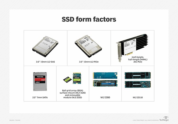
- Flash Memory: Non-volatile, used in solid-state drives (SSDs) and USB drives.
22. How Temperature Affects Semiconductor Performance
Temperature can significantly affect semiconductor performance:
- High Temperatures: Can increase leakage current, reduce carrier mobility, and degrade reliability.
- Low Temperatures: Can reduce carrier mobility and affect the switching speed of transistors.
23. Semiconductor Reliability: Ensuring Long-Term Performance
Semiconductor reliability is crucial for ensuring long-term performance. Factors that affect reliability include:
- Thermal Stress: Caused by temperature variations.
- Electrical Stress: Caused by high voltages and currents.
- Mechanical Stress: Caused by physical forces.
- Radiation Effects: Caused by exposure to radiation.
24. The Role of Semiconductors in Telecommunications
Semiconductors are essential for modern telecommunications:
- Mobile Phones: Use semiconductors for signal processing, amplification, and switching.
- Wireless Networks: Rely on semiconductors for base stations and wireless devices.
- Fiber Optic Communication: Use semiconductors for lasers and photodetectors.
- Satellite Communication: Use semiconductors for transponders and ground stations.
25. Semiconductor Packaging: Protecting and Connecting the Chip
Semiconductor packaging is the process of encasing the chip in protective materials and providing electrical connections to the outside world. Key packaging technologies include:
- Wire Bonding: Connecting the chip to the package using thin wires.
- Flip Chip: Mounting the chip upside down on the package.
- Through-Silicon Vias (TSVs): Creating vertical connections through the silicon die.
26. What are Compound Semiconductors?
Compound semiconductors are made from two or more elements, offering unique properties compared to silicon:
- Gallium Arsenide (GaAs): High electron mobility, used in high-frequency applications.
- Indium Phosphide (InP): High electron velocity, used in optical communication.
- Silicon Carbide (SiC): High breakdown voltage, used in power electronics.
- Gallium Nitride (GaN): High power and high-frequency capabilities, used in RF and power applications.
27. What is an FPGA (Field-Programmable Gate Array)?
An FPGA is a type of semiconductor that can be reprogrammed after manufacturing. FPGAs are used in a wide range of applications, including:
- Aerospace and Defense: Signal processing and hardware acceleration.
- Automotive: Advanced driver-assistance systems (ADAS).
- Data Centers: Network acceleration and customized computing.
- Industrial Automation: Motor control and robotics.
28. What is an ASIC (Application-Specific Integrated Circuit)?
An ASIC is a semiconductor designed for a specific application. ASICs offer high performance and efficiency but are more expensive and time-consuming to develop than FPGAs. They are used in applications such as:
- Consumer Electronics: Mobile phones and gaming consoles.
- Automotive: Engine control and infotainment systems.
- Telecommunications: Network processors and switches.
- Data Centers: Specialized computing and acceleration.
29. The Role of Semiconductors in Artificial Intelligence (AI)
Semiconductors are essential for AI applications:
- GPUs (Graphics Processing Units): Used for training AI models due to their parallel processing capabilities.
- TPUs (Tensor Processing Units): Custom-designed by Google for AI workloads.
- AI Accelerators: Specialized chips designed to accelerate AI tasks such as image recognition and natural language processing.
30. Future Trends in Semiconductor Technology
- More-than-Moore: Integrating different functionalities onto a single chip beyond transistor scaling.
- Chiplets: Assembling multiple smaller chips into a single package to improve performance and flexibility.
- Heterogeneous Integration: Combining different materials and technologies on a single chip.
- Quantum Computing: Developing semiconductors for quantum computers, which promise revolutionary processing power.
- Neuromorphic Computing: Creating chips that mimic the human brain for AI applications.
31. Impact of IoT (Internet of Things) on Semiconductors
The proliferation of IoT devices is driving demand for semiconductors:
- Microcontrollers: Used to control and manage IoT devices.
- Sensors: Collect data from the environment.
- Connectivity Chips: Enable communication between IoT devices and the cloud.
- Low-Power Semiconductors: Extend battery life in IoT devices.
32. Semiconductor Materials Beyond Silicon: Graphene and More
Researchers are exploring alternative materials to silicon:
- Graphene: A single layer of carbon atoms with high electron mobility and thermal conductivity.
- Carbon Nanotubes: Cylindrical structures with unique electrical and mechanical properties.
- Transition Metal Dichalcogenides (TMDs): Layered materials with tunable electronic properties.
33. Challenges and Opportunities in Advanced Semiconductor Packaging
Advanced packaging technologies are critical for improving performance and density:
- 3D Packaging: Stacking chips vertically to increase density and performance.
- Fan-Out Wafer-Level Packaging (FOWLP): Embedding chips in a mold compound and creating connections on the surface.
- Silicon Interposers: Using silicon substrates to create high-density interconnects between chips.
34. Semiconductor Testing: Ensuring Quality and Reliability
Semiconductor testing is crucial for ensuring quality and reliability. Key testing methods include:
- Wafer Probing: Testing individual chips on the wafer before packaging.
- Functional Testing: Verifying that the chip performs its intended functions.
- Stress Testing: Subjecting the chip to extreme conditions to assess its reliability.
- Burn-In Testing: Operating the chip at elevated temperatures to accelerate failure mechanisms.
35. The Future of Semiconductor Manufacturing Equipment
The future of semiconductor manufacturing equipment will be driven by the need for higher precision, throughput, and efficiency:
- Extreme Ultraviolet (EUV) Lithography: Using shorter wavelengths of light to create smaller features.
- Directed Self-Assembly (DSA): Using chemical processes to create self-assembling patterns.
- Atomic Layer Deposition (ALD): Depositing thin layers of materials with atomic-level precision.
- Advanced Metrology Tools: Measuring and inspecting wafers with higher resolution and accuracy.
36. Addressing the Semiconductor Skills Gap
The semiconductor industry faces a growing skills gap:
- Education and Training: Investing in education and training programs to develop skilled workers.
- Industry Collaboration: Partnering with universities and research institutions to advance semiconductor technology.
- Recruitment and Retention: Attracting and retaining talented employees.
- Diversity and Inclusion: Promoting diversity and inclusion in the semiconductor workforce.
37. Semiconductor Intellectual Property (IP) and Design
Semiconductor IP refers to reusable design blocks that can be integrated into custom chips. Key types of IP include:
- Processor Cores: Central processing units (CPUs) and microcontrollers.
- Memory Controllers: Interfaces for accessing different types of memory.
- Connectivity Interfaces: Interfaces for connecting to peripherals and networks.
- Analog and Mixed-Signal Blocks: Circuits for signal conditioning and data conversion.
38. What is Silicon Photonics?
Silicon photonics combines silicon microelectronics with optical devices to create high-speed, low-power communication links. Key applications include:
- Data Centers: Interconnecting servers and networking equipment.
- High-Performance Computing: Enabling faster communication between processors and memory.
- Optical Transceivers: Converting electrical signals to optical signals and vice versa.
39. The Role of Government in the Semiconductor Industry
Governments play a crucial role in supporting the semiconductor industry:
- Research and Development Funding: Investing in basic and applied research.
- Tax Incentives: Encouraging companies to invest in manufacturing and R&D.
- Trade Policies: Promoting fair trade and protecting intellectual property.
- Workforce Development: Supporting education and training programs.
40. Understanding Semiconductor Device Fabrication
Device fabrication involves various processes:
- Wafer Preparation: Cleaning and preparing the silicon wafer.
- Thin Film Deposition: Depositing thin layers of materials.
- Lithography: Transferring patterns onto the wafer.
- Etching: Removing unwanted material.
- Doping: Introducing impurities.
- Metallization: Creating electrical contacts.
41. Different Types of Semiconductor Memories
- ROM (Read-Only Memory): Non-volatile, used for storing firmware and boot code.
- PROM (Programmable ROM): Can be programmed once by the user.
- EPROM (Erasable PROM): Can be erased and reprogrammed using ultraviolet light.
- EEPROM (Electrically Erasable PROM): Can be erased and reprogrammed electrically.
- NVRAM (Non-Volatile RAM): Combines SRAM with non-volatile memory for data retention.
42. Emerging Semiconductor Technologies
- 3D NAND Flash Memory: Stacking memory cells vertically to increase density.
- Resistive RAM (ReRAM): Using materials that change resistance based on applied voltage.
- Magnetoresistive RAM (MRAM): Using magnetic materials to store data.
- Ferroelectric RAM (FeRAM): Using ferroelectric materials to store data.
43. Semiconductor Failure Mechanisms
Semiconductor devices can fail due to various mechanisms:
- Electromigration: Migration of metal atoms due to high current densities.
- Hot Carrier Injection: Injection of high-energy carriers into the gate oxide.
- Time-Dependent Dielectric Breakdown (TDDB): Degradation of the gate oxide over time.
- Stress Migration: Migration of atoms due to mechanical stress.
- Corrosion: Degradation of materials due to chemical reactions.
44. Semiconductor Market Segmentation
The semiconductor market is segmented by:
- Product Type: Integrated circuits, discrete devices, optical semiconductors, and sensors.
- Application: Consumer electronics, automotive, industrial, communications, and healthcare.
- Geography: North America, Europe, Asia-Pacific, and Rest of the World.
45. The Impact of Semiconductor Shortages on Various Industries
Semiconductor shortages have had a significant impact on various industries:
- Automotive: Reduced production due to lack of chips for engine control and infotainment systems.
- Consumer Electronics: Delays in the production of smartphones, laptops, and gaming consoles.
- Industrial Automation: Disruptions in the supply chain for industrial equipment and machinery.
- Healthcare: Shortages of medical devices and diagnostic equipment.
46. How to Choose the Right Semiconductor for Your Application
Choosing the right semiconductor depends on several factors:
- Performance Requirements: Speed, power consumption, and operating frequency.
- Environmental Conditions: Temperature, humidity, and radiation levels.
- Reliability Requirements: Expected lifetime and failure rate.
- Cost Constraints: Budget limitations.
- Availability and Lead Time: Time required to procure the semiconductor.
47. The Role of AI in Semiconductor Design and Manufacturing
AI is transforming semiconductor design and manufacturing:
- Design Automation: Using AI to optimize circuit layouts and reduce design time.
- Process Control: Using AI to monitor and control manufacturing processes.
- Defect Detection: Using AI to identify and classify defects in wafers.
- Predictive Maintenance: Using AI to predict equipment failures and optimize maintenance schedules.
48. Understanding CMOS (Complementary Metal-Oxide-Semiconductor) Technology
CMOS is the dominant technology used in modern integrated circuits. Key features include:
- Low Power Consumption: Consumes power only during switching.
- High Noise Immunity: Resistant to noise and interference.
- Scalability: Can be scaled down to smaller feature sizes.
- Versatility: Can be used for both digital and analog circuits.
49. The Importance of Thermal Management in Semiconductor Devices
Thermal management is crucial for ensuring reliable operation:
- Heat Sinks: Used to dissipate heat from the chip.
- Fans: Used to force air over the heat sink.
- Liquid Cooling: Using liquids to remove heat from the chip.
- Thermoelectric Coolers (TECs): Using the Peltier effect to cool the chip.
50. What are Power Semiconductors?
Power semiconductors are used to control and switch high voltages and currents. Key types include:
- Power Diodes: Used for rectification and voltage regulation.
- Power Transistors: Used for switching and amplification.
- Thyristors: Used for high-power switching applications.
- Insulated Gate Bipolar Transistors (IGBTs): Combine the features of MOSFETs and bipolar transistors.
Ready to dive deeper into the world of semiconductors? Don’t let your curiosity wait! Visit WHAT.EDU.VN today and ask any question you have. Our community of experts is here to provide you with fast, accurate, and free answers. Contact us at 888 Question City Plaza, Seattle, WA 98101, United States. Whatsapp: +1 (206) 555-7890. Website: what.edu.vn. Your quest for knowledge starts here! Let’s unlock the power of understanding together!